Microstructures under a scanning electron microscope (SEM)
Transforming smooth polymer into a functional surface through etching
The component shape, roughness, and waviness are key factors in the surface topography of technical components. Surface topography has a significant influence on tribological properties, such as wear and friction, as well as haptics—that is, the sensation and perception of the surface—and aesthetics, which are strongly influenced by gloss and color.
For plastic components, surface properties—specifically surface topography—play a crucial role in adhesion and coating processes. For example, in the automotive and electronics industries, plastic surfaces are intentionally roughened to improve adhesion in adhesive bonds. Surface topography is also important in painting and coating processes to ensure the adhesion of the coating system as well as the flow and appearance of the coating.
The etching process is an established chemical method for modifying surfaces, in which surfaces are specifically altered through the use of etching solutions. The objectives range from creating a roughened surface to generating porosity to the selective attack of individual areas (molecules).
Translated with DeepL.com (free version)
Surface etching is a typical pretreatment step prior to electroplating, painting, coating, bonding, and printing on surfaces. Not all plastics are suitable for this process. In practice, ABS (acrylonitrile butadiene styrene copolymer), PC/ABS (polycarbonate-ABS copolymer), or PA (polyamide) are commonly used.
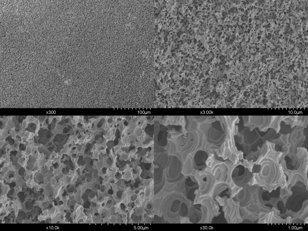
Evaluation of the topography using scanning electron microscopy (SEM)
Appropriate analytical methods are necessary to evaluate the surface structures produced by etching. This is particularly relevant for quality assurance of etching processes, but also for research questions regarding the influence of topography on material behavior. However, microscopic methods (optical microscopy and digital microscopy) are insufficient for evaluation due to their limited resolution and depth of field in the micro- and nanometer range.
The scanning electron microscope (SEM) enables detailed imaging of such surface structures at the micro- and nanometer scales with high depth of field and resolution. Unlike light microscopy techniques, scanning electron microscopy is based on the interaction of electrons with the surface being examined. The advantage is that even the smallest topographical differences become visible.
Please contact us to learn more about our work in surface analysis as well as materials and failure analysis. We would be happy to provide you with practical application examples related to these fields.
